
How SMD Screens are Manufactured: A Behind-the-Scenes Look
As technology continues to advance at a rapid pace, one marvel of modern engineering that has seamlessly integrated into our everyday lives is SMD screens. From smartphones and laptops to billboards and televisions, these sleek, high-definition screens have become ubiquitous. However, have you ever wondered how these mesmerizing displays are manufactured? In this article, we will take you behind the scenes of SMD screen production, delving into the intricate processes and cutting-edge techniques that bring these stunning visuals to life. Join us on this informative journey as we unveil the secrets of SMD screen manufacturing, providing a professional insight into the fascinating world that lies beneath the surface.
Table of Contents
- 1. Understanding the Design and Components of SMD Screens: Decoding the Complex Architecture
- 2. Unraveling the Intricate Manufacturing Process: From PCB Assembly to Soldering Techniques
- 3. Ensuring Quality and Reliability: Testing and Inspection Procedures for SMD Screens
- 4. Best Practices and Future Trends: Key Recommendations for SMD Screen Manufacturers
- Q&A
- Wrapping Up
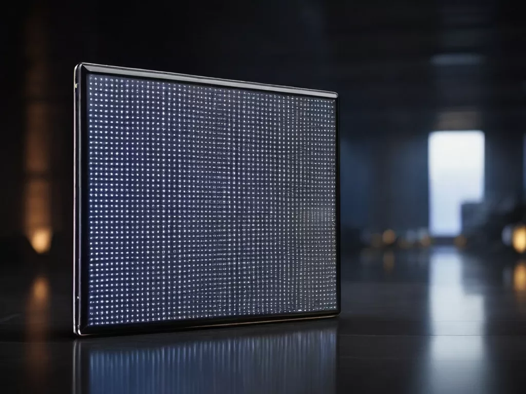
1. Understanding the Design and Components of SMD Screens: Decoding the Complex Architecture
When it comes to the world of LED displays, Surface Mount Display (SMD) screens are truly a marvel of modern technology. These screens are not only high-resolution and vibrant but also incredibly compact and durable. In this post, we will delve into the intricate design and components that make up these SMD screens, offering you a behind-the-scenes look at how they are manufactured.
1. Encapsulation
- SMD screens consist of hundreds or even thousands of tiny LED chips, typically made of GaN (Gallium Nitride) or InGaN (Indium Gallium Nitride) materials. These chips are encapsulated using a special epoxy resin, ensuring their protection from external elements like moisture and dust.
- This encapsulation process is crucial to the longevity of the screen, as it enhances its resistance to environmental factors, making it suitable for both indoor and outdoor installations.
2. PCB (Printed Circuit Board)
- The heart of any SMD screen is the Printed Circuit Board (PCB) where the LED chips are mounted. The PCB acts as a platform to connect the various components of the display system.
- Using advanced manufacturing techniques, multiple layers of copper and insulating material are etched onto the PCB, creating a complex network of electrical pathways.
| Component | Material | Function |
|---|---|---|
| Microcontroller | Silicon | Controls the display’s operation and functions |
| Driver ICs | Semiconductor | Translates the video signal into the correct format for the LED chips |
| Power Supply | Electronic components | Converts AC power to the required DC voltage for the screen |
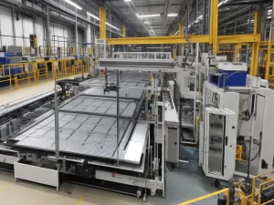
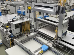
2. Unraveling the Intricate Manufacturing Process: From PCB Assembly to Soldering Techniques
In the fast-paced world of technology, SMD screens have become an integral part of our daily lives. These sleek and thin displays are found in a wide range of devices, from smartphones to televisions. But have you ever wondered how these screens are manufactured? In this post, we will take you behind the scenes of the intricate manufacturing process involved in creating SMD screens.
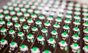
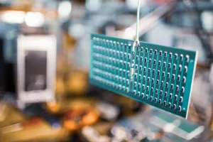
The journey of manufacturing an SMD screen begins with the Printed Circuit Board (PCB) assembly. This is where all the electronic components are mounted onto the PCB, creating a solid foundation for the screen. The components are carefully picked and placed on the board using state-of-the-art machinery, ensuring precise alignment and accuracy. Soldering techniques are employed to securely bond the components to the PCB, creating a reliable connection. Advanced surface mount technology (SMT) is used, allowing for high-density placement and minimizing the size of the screen. This process is crucial in achieving the thin and lightweight design that SMD screens are known for.
To further enhance the quality of the SMD screen, a specialized bonding process is employed. This involves attaching a thin layer of adhesive material between the screen and the PCB. The adhesive ensures a strong bond, preventing any potential detachment or damage. The screen is then carefully aligned and pressed onto the PCB, creating a solid connection. Once the bonding process is complete, electrical tests are conducted to ensure that each screen functions properly. This rigorous quality control ensures that only the highest quality SMD screens make it to the market.
Manufacturing SMD screens is a meticulous and intricate process that requires a blend of advanced technology, skilled craftsmanship, and rigorous quality control. From the PCB assembly to the soldering techniques, each step is meticulously performed to create screens that deliver exceptional visual experiences. So the next time you use a device with an SMD screen, take a moment to appreciate the craftsmanship and attention to detail that went into its creation.
3. Ensuring Quality and Reliability: Testing and Inspection Procedures for SMD Screens
Ensuring quality and reliability is a crucial step in the manufacturing process of SMD screens. Testing and inspection procedures play a vital role in guaranteeing that the screens meet the highest standards before they are shipped out to customers. This behind-the-scenes look will give you an insight into the meticulous processes involved in this aspect of SMD screen production.
One of the key testing procedures performed on SMD screens is the visual inspection. Expert technicians carefully examine each screen for any defects such as dead pixels, color irregularities, or physical damages. This meticulous inspection ensures that only screens of the highest quality move forward in the production process. In addition to the visual inspection, electronic testing is conducted to evaluate the functional capabilities of the screens. This involves analyzing various parameters such as brightness, contrast, color accuracy, and response time to ensure optimal performance.
In addition to these inspection procedures, SMD screens undergo environmental testing to assess their reliability and durability. They are subjected to extreme temperatures, humidity, and vibration to ensure they can withstand various environmental conditions without compromising performance. This extensive testing process guarantees that the screens are reliable and can deliver exceptional visual experiences consistently.
| Testing Procedure | Parameters Evaluated |
|---|---|
| Visual Inspection | Defects such as dead pixels, color irregularities, and physical damages |
| Electronics Testing | Brightness, contrast, color accuracy, and response time |
| Environmental Testing | Reliability and durability under extreme temperatures, humidity, and vibration |
4. Best Practices and Future Trends: Key Recommendations for SMD Screen Manufacturers
As the demand for SMD (Surface Mount Device) screens continues to rise, it is crucial for manufacturers to stay ahead of the game by implementing best practices and keeping an eye on future trends. By following these key recommendations, manufacturers can enhance their production processes, improve product quality, and remain competitive in the ever-evolving market.
1. Implement Advanced Quality Control Systems:
Investing in state-of-the-art quality control systems is essential for ensuring that every SMD screen leaving the production line meets the highest standards. By meticulously monitoring the soldering process, component placement, and alignment accuracy, manufacturers can detect any defects or errors early on and prevent them from reaching the market. This not only helps deliver top-notch products but also reduces costly rework and improves customer satisfaction.
2. Embrace Energy-efficient Technologies:
With the increasing emphasis on sustainability and energy efficiency, integrating energy-saving technologies into SMD screen manufacturing is paramount. Manufacturers should explore the use of LEDs with low power consumption, optimize power management systems, and ensure efficient heat dissipation. This not only reflects a commitment to environmental responsibility but also appeals to customers who prioritize energy-saving products. Furthermore, embracing energy-efficient technologies can lead to long-term cost savings for both manufacturers and end-users.
3. Stay Up-to-date with Advancements in Materials:
Materials play a crucial role in the overall performance and durability of SMD screens. Manufacturers should continuously research and test new materials that offer improved reliability, color accuracy, and resistance to physical and chemical damage. For example, incorporating strengthened glass with enhanced scratch resistance and exploring alternative materials for backlighting can greatly enhance the quality and longevity of the screens.
4. Consider Flexibility and Customization Options:
In today’s fast-paced market, customers often require screens that can be tailored to their specific needs. Manufacturers should focus on offering flexible solutions and customization options that allow for various screen sizes, aspect ratios, and resolutions. This approach not only attracts a wider customer base but also enables manufacturers to adapt quickly to changing market demands.
5. Emphasize Collaboration and Knowledge Exchange:
Collaboration with industry experts, research institutions, and customers is essential for manufacturers to stay at the forefront of SMD screen technology. By actively participating in conferences, knowledge-sharing platforms, and partnerships, manufacturers can gain access to the latest research, trends, and innovations. This collaborative approach fosters a culture of continuous improvement and promotes the development of cutting-edge products.
Q&A
Q: What is the manufacturing process of SMD screens?
A: The manufacturing process of SMD (Surface-Mount Device) screens involves several intricate steps to create the final product we see in our electronic devices.
Q: Can you explain the initial stage of SMD screen manufacturing?
A: The first stage in SMD screen manufacturing is the selection and preparation of raw materials. This includes sourcing high-quality substrates, such as glass or metal, which serve as the foundation for the screen.
Q: What happens next in the manufacturing process?
A: Once the raw materials are prepared, the substrate goes through a meticulous cleaning process to ensure its surface is free from impurities. This step is crucial as any contaminants can impact the display quality.
Q: Could you shed some light on the creation of the electronic circuit?
A: Certainly. To create the electronic circuit, a thin layer of conductive material, like Indium Tin Oxide (ITO), is deposited onto the substrate. This layer acts as a conductor, enabling the transmission of electrical signals throughout the screen.
Q: How are pixels formed in SMD screens?
A: The manufacturing process then moves on to forming pixels. Tiny red, green, and blue (RGB) diodes are placed on the substrate using a technique called pick-and-place or surface mounting. Each diode corresponds to one pixel on the screen.
Q: After placing RGB diodes, what additional steps are involved?
A: After the diodes are placed, a protective layer, known as the encapsulation layer, is added. This layer safeguards the diodes from external damage and helps maintain color accuracy and consistency.
Q: How are pixels controlled to produce images?
A: Once all the components are in place, electrical connections are established using a network of conducting materials. These connections serve as pathways for controlling the individual pixels, allowing them to display the desired images.
Q: What happens post-assembly of the SMD screens?
A: Post-assembly, the screens undergo rigorous testing for functionality and quality assurance. This ensures that each screen meets the required standards and performs as intended.
Q: Are there any intricacies or challenges in the manufacturing process?
A: Absolutely. The manufacturing process of SMD screens demands a high level of precision and accuracy. Minimizing defects, such as dead pixels or faulty connections, is crucial to avoid compromising the overall display quality.
Q: Can you provide an overview of advancements in SMD screen manufacturing?
A: Over the years, advancements in manufacturing technology have led to more efficient production processes. Innovations like ultra-thin substrates, higher pixel densities, and improved color reproduction have greatly enhanced the quality of SMD screens.
Q: Any final thoughts on the manufacturing of SMD screens?
A: The production of SMD screens involves a meticulous and precise process, requiring advanced technologies and expertise. Understanding the behind-the-scenes manufacturing provides a deeper appreciation for the screens that are an integral part of our daily lives.
Wrapping Up (How SMD Screens are Manufactured)
In conclusion, taking a behind-the-scenes look into the manufacturing process of SMD screens has provided us with invaluable insights into the intricate and meticulous world of modern display technology. From their inception as a mere concept to the fully-fledged screens that grace our lives today, numerous stages of innovation, precision engineering, and rigorous quality control measures are undertaken.
The journey begins with the design and development phase, where cutting-edge technology is harnessed to create intricate circuitry patterns on ultra-thin substrates. The delicate process of surface mounting components onto these miniaturized modules follow, requiring highly skilled technicians and state-of-the-art machinery.
Next, the modules undergo a series of testing and inspection procedures to ensure they meet stringent industry standards for performance and durability. Any discrepancies are promptly addressed to guarantee optimal functionality across a wide range of environmental conditions.
The fabrication of these miniature marvels continues with the assembly of the modules onto robust and reliable backplanes. The seamless integration of the various parts, including drive electronics and control systems, forms a cohesive unit capable of delivering breathtaking visual experiences.
Finally, we unveil the encapsulation process, where the encapsulant material is precisely applied to achieve the desired level of protection and optical efficiency. Advanced techniques such as automatic optical inspection (AOI) and solder paste printing guarantee the precision and accuracy required in this critical step.
As we conclude this journey through the manufacturing of SMD screens, we are left with an appreciation for the meticulous craftsmanship that brings these technologically advanced devices to life. The remarkable dedication of engineers and technicians, coupled with cutting-edge machinery and rigorous quality control protocols, ensure that the screens we use every day set the industry benchmark for excellence.
Understanding the intricacies and complexities involved in the creation of SMD screens not only enhances our appreciation for the final product but also offers a glimpse into the future of display technology. With relentless innovation and the pursuit of perfection, we can expect even more astonishing developments in the realm of SMD screens, transforming our visual experiences and revolutionizing various industries in the years to come.
Looking for premium SMD screens and professional display solutions? SMDLED.PK is your trusted partner for state-of-the-art SMD technology. Explore our top-quality products like the stunning Leyard HDR 4K SMD Video Wall for crystal-clear visuals, the versatile MSA Plus SMD LED Screen Module, the sleek MSA Ultra Thin SMD LED Screen Module for modern setups, the durable MSG Outdoor SMD LED Screen Module, and the efficient MSG Indoor SMD LED Screen Module perfect for indoor environments.
We also offer exceptional Outdoor SMD Screens, Indoor SMD Screens, Flexible SMD Screens for creative designs, Cabinet SMD Screens for secure setups, Signpole SMD Screens for advertising, and stunning SMD Video Walls for large-scale visual impact. With SMDLED.PK, experience reliability, superior technology, and tailored solutions for all your display needs. Visit us today and transform your spaces with unparalleled visual excellence!
How SMD Screens are Manufactured: A Behind-the-Scenes Look of SMD Screen Manufacturing
Contact Us For Free Consultation at 0306-1333384
Powered By BIACommunication